
In the last few sections methods of transmitting analog information using analog signals were explained. This section will consider methods of transmitting digital data using analog signals.
The most familiar use of these methods is in data communications, where modems and telephone networks are used; because integrated circuits are generally used a block diagram approach will be considered.
19.7.1 Frequency Shift Keying
In some situations data can be transmitted directly without any modulation technique being necessary. This is applicable over short distances where the baseband signal may be sent in a raw form. However, where distance is involved more sophisticated methods are required.
One of the modulation methods most frequently used is frequency shift keying (FSK). In FSK the transmitted signal is switched between two frequencies every time there is a change in the level of the modulating data stream. The higher frequency may be used to represent a high level (1) and the lower frequency used for the low level (0). This results in a waveform similar to the one shown in Figure 19.21.
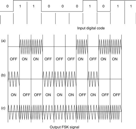
Figure 19.21 Frequency shift keying
Generally the frequencies used in FSK depend on the system application. Most modems traditionally use frequencies within the voice range (300–3400 Hz), while much higher frequencies would be used for satellite or radio relay systems. No matter what system is used there are fundamental blocks which are necessary for successful operation.
A balanced modulator is necessary to generate the required waveforms. This device has been mentioned earlier; it simply multiplies two signals together at its two inputs, the output voltage being the product of these two voltages. One of the inputs (the carrier input) is generally AC coupled, while the other (the digital data input) is DC coupled. The block diagram is shown in Figure 19.22. Note that the data stream is inverted in modulator 2 in order to switch to the second carrier frequency.
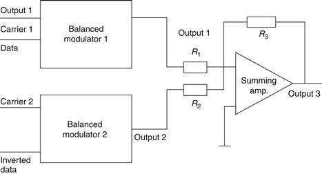
Figure 19.22 Block diagram showing balanced modulator
At the receiver end, the FSK waveform has to be demodulated or, more specifically, decoded. One approach used for this is shown in Figure 19.23. The demodulation of FSK signals can be accomplished by means of a ratio detector or a PLL, but for modem applications the PLL is generally preferred as it can be used for both modulation and demodulation. The data stream consists of marks (1) and spaces (0) which are each allocated a switched frequency. The space is normally allocated the higher frequency. The rate at which the carrier frequency is switched is known as the baud rate, and this is the same as the digital data rate for FSK. This is not always the case for other demodulation methods. The PLL has a free running frequency of its own and this is normally set between the mark and space carriers when designing such a system.
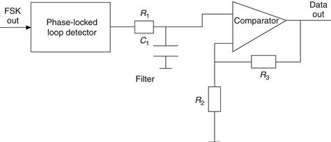
Figure 19.23 Demodulation of FSK waveform
The output of the PLL in Figure 19.23 contains numerous components due to the interaction of the two frequencies, and hence a low-pass filter is used. However, the output of the filter produces rounded waveforms instead of oblong-shaped pulses, and this is modified by including a comparator.
Example 19.12
An FSK receiver uses a PLL as part of its demodulation circuitry, to receive digital data at the rate of 1200 bps. If the mark frequency is 1 kHz and the space frequency is 1.72 kHz, determine:
(a) the free running frequency of the PLL,
(b) the bandwidth of the receiver.
Solution
(a) Since the mark and space carriers are separated by 720 Hz, the centre frequency is 1.36 kHz and this will be the free running frequency of the VCO in the PLL.
(b) Since the data rate is 1200 bps, the frequency is 600 Hz. Also the input to the PLL has to swing between 1 kHz and 1.72 kHz, i.e., ±360 Hz. The deviation ratio is thus:

From the Bessel tables,

Hence, two side frequencies are available and the bandwidth is:

This falls within the baseband range of 300–3400 Hz, and the output will use a filter and comparator as shown in Figure 19.23.
19.7.2 Binary Phase-Shift Keying (BPSK)
High-speed modems operating at bit rates of up to 56 kbps require phase-shift keying or quadrature phase-shift keying. It is also the preferred modulation method for satellite and space technology. Unlike FSK, phase-shift keying uses one carrier frequency which is modulated by the data stream. It is a modulation system in which only discrete phase states are allowed. Usually 2n phase states are used, and when n=1 this gives two-phase changes. This is sometimes called binary phase-shift keying (BPSK). When n=2, four phase changes are produced, and this is called quadrature phase-shift keying (QPSK).
BPSK (Figure 19.24), which will be considered here, is a two-phase modulation method in which a carrier is transmitted to indicate a mark (1) or the phase is reversed (shifted through 180°) to indicate a space (0). Note that the phase shift does not have to be 180°, but this allows for the maximum separation of the digital states between 1 and 0, which is important when noise is prevalent.
Figure 19.24 Binary phase-shift keying (BPSK)
The block diagram shown in Figure 19.25 indicates the stages necessary to produce the modulator section. A balanced modulator is used with the carrier applied as shown. The digital input passes through a unipolar-bipolar convertor to ensure that the digital signal passed to the balanced modulator is unipolar.
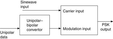
Figure 19.25 Block diagram showing stages to produce modulator section
It can be seen from Figure 19.24 that when the modulation input is positive, the modulator multiplies the carrier input by this constant positive level so that the output signal is simply the carrier sine wave. Note this is in phase with the carrier input. When the digital input data is negative, the modulator multiplies the carrier input by this constant negative level. This causes an output sine wave which is 180° out of phase with the carrier input. The result is that the sine wave at the output is inverted in phase every time the data input changes and produces a transition from 1 to 0 or 0 to 1. The consequence of this action is that the sine wave is inverted each time the modulation input undergoes a transition.
In order to demodulate a BPSK waveform, the demodulator must have an internal signal whose frequency is exactly equal to the incoming carrier. The PLL on its own is unsuitable in this case because of the sudden phase reversals which cannot produce a discrete carrier component to lock on to. One circuit which overcomes this is shown in Figure 19.26.
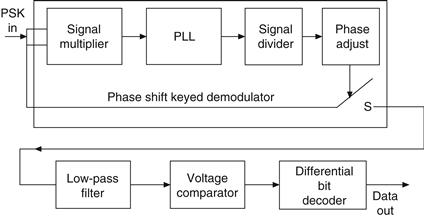
Figure 19.26 Circuit to demodulate a BPSK waveform
The input signal is applied to a signal multiplier which is a square-law device. In this case a balanced demodulator is used, with its inputs tied together. The output from this stage is a signal at twice the original frequency and having phase changes of 0° and 360°. Hence the signal multiplier has removed any phase changes from the original BPSK signal. It now provides a signal which the PLL can lock on to. The output from the PLL is then passed to a divide-by-two network which produces the original BPSK signal. The phase of this signal is then adjusted to the phase of the original BPSK signal. Finally, this output is used to activate an FET switch. When the phase adjust output is high (1) the switch is closed, and the initial BPSK signal is switched through to the demodulator’s output. If the phase adjust output is low (0) then the switch is open and the demodulator’s output drops to ground potential.
The output is then passed to a low-pass filter to remove unwanted signal components. This is followed by a comparator which squares the output and produces clean positive and negative half-cycles.
One final stage is necessary in order to produce the original data. At the output of the comparator the receiver has to look for level changes, and this has to be done by a differential decoder block which gives an output (1) when a level change is sensed and no output (0) when no level change takes place. Hence, the original data stream is reproduced.
19.7.3 Quadrature Phase-Shift Keying (QPSK)
This type of modulation method has wide application in high-speed data transmission systems. It has two distinct advantages: it produces twice as much data with the same number of phase changes as BPSK, and this also means that the bandwidth is virtually decreased for the same amount of data being transmitted. In order to understand this, it is informative to look at single sideband modulation, which was mentioned in section 19.2.
In quadrature phase-shift keying each pair of consecutive data bits in a data stream is considered a two-bit code called a dibit. This is used to switch the carrier at the transmitter between one of four phases, instead of two as was the case with BPSK. The phases selected are 45°, 135°, 225° and 315°, lagging relative to the phase of the original unmodulated carrier. The system is shown in Figure 19.27. This diagram is clarified by looking at the typical QPSK transmitter block diagram shown in Figure 19.28.
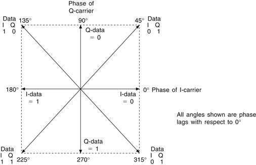
Figure 19.27 Quadrature phase-shift keying
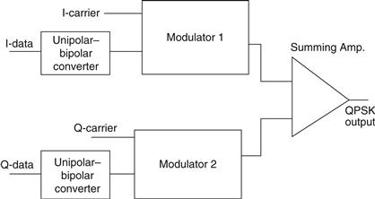
Figure 19.28 Typical QPSK transmitter block diagram
The two carrier signals shown in Figure 19.28 have the same frequency but differ in phase by 90°. The 0° phase carrier is called the in-phase (I) carrier, while the 90° phase carrier is called the quadrature (Q) carrier. The output from the first modulator is a BPSK signal which has phases of 0° and 90° relative to the I carrier while the output of the second modulator is a BPSK signal with phases of 90° and 270° relative to the I carrier. These two signals are then applied to the summing amplifier, but note that there is always ±90° phase difference between the two modulator outputs.
The phase of the summing amplifier’s output, relative to the I carrier, can take one of four phase values as shown in Figure 19.26, but this will depend on the dibit code applied to the balanced modulator inputs. When the dibit changes, the phase of the QPSK output changes by 0°, 90°, 180° or 270° from its previous phase position.
It is necessary to include a differentially encoded dibit (DED) sequence at the transmitter in order to avoid phase ambiguity at the receiver. In order to achieve this, two blocks are connected at the input of the unipolar–bipolar converters of Figure 19.28. These blocks cause each pair of consecutive dibits from the data stream to be encoded as a change in the code at the two outputs of the DED. These outputs are then used to drive the modulator inputs and the original dibits cause the appropriate phase changes.
As with the BPSK receiver, the circuitry is fairly complicated but integrated circuitry enables the block diagram of Figure 19.29 to be drawn.
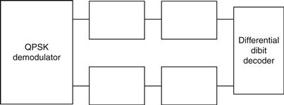
Figure 19.29 Block diagram of QPSK using integrated circuitry
The QPSK signal goes to the first stage of the QPSK demodulator, which is a signal squarer. This multiplies the incoming signal by itself causing phase changes of 0° and 180°. (The four original phase changes have been doubled.) The output from this block is then passed on to a second signal squarer and the output from this stage only incorporates a single phase change of 0°, but the frequency is now four times the original. The next stage is a PLL, which locks on to the incoming signal and outputs a clean square wave. This output is then passed to a divide-by-four circuit which outputs the original frequency and passes it on to a phase-changing circuit which generates two square waves at the same frequency but separated by a 90° phase difference. Finally, these outputs are used to operate two FET switches so that when the output is high one switch is closed and the original QPSK signal passes through to the demodulator. If the output is low, one of the FET switches will open and the demodulator input drops to zero.
Figure 19.27 shows how the outputs from the demodulator are arranged with reference to the I and Q signals. Note that the information concerning the original dibit code is incorporated in the average levels of the demodulator’s I and Q outputs, hence low-pass filtering is used next to extract the average levels. This is then passed on to two voltage comparators to produce clean square waves. Finally, the change in the dibit code is determined by the differential dibit decoder, which encodes this change as the original dibit pair.
Leave a Reply