More complex components called transistors can be created by forming a sandwich out of three regions of doped silicon. One family of transistors is known as bipolar junction transistors (BJTs) of which there are two basic types called NPN and PNP; these names relate to the way in which the silicon is doped (Figure 10.5).
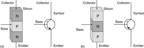
Figure 10.5 Bipolar junction transistors (BJTs); (a) NPN bipolar junction transistor; (b) PNP bipolar junction transistor
In the analog world, a transistor can be used as a voltage amplifier, a current amplifier, or a switch; in the digital world, a transistor is primarily considered to be a switch. The structure of a transistor between the collector and emitter terminals is similar to that of two diodes connected back-to-back. Two diodes connected in this way would typically not conduct; however, when signals are applied to the base terminal, the transistor can be turned ON or OFF. If the transistor is turned ON, it acts like a CLOSED switch and allows current to flow between the collector and the emitter; if the transistor is turned OFF, it acts like an OPEN switch and no current flows. We may think of the collector and emitter as data terminals, and the base as the control terminal.
As for a diode, an individually packaged transistor consists of the silicon, with connections to external leads, all encapsulated in a protective package (the silicon is typically smaller than a grain of sand). The package protects the silicon from moisture and other impurities and helps to conduct heat away from the silicon when the transistor is operating. Transistors may be packaged in plastic or in little metal cans about a quarter of an inch in diameter with three leads sticking out of the bottom (Figure 10.6).
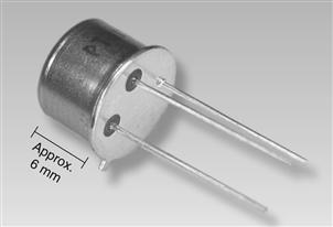
Figure 10.6 Individually packaged transistor (photo courtesy of Alan Winstanley)
Leave a Reply