
To illustrate the application of a transistor as a switch, first consider a simple circuit comprising a resistor and a real switch (Figure 10.8).
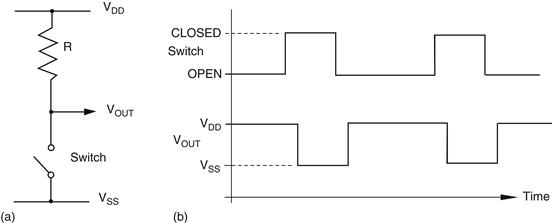
Figure 10.8 Resistor-switch circuit (a) Circuit; (b) Waveform
The labels VDD and VSS are commonly used in circuits employing MOSFETs. At this point we have little interest in their actual values and, for the purpose of these examples, need only assume that VDD is more positive than VSS.
When the switch is OPEN (OFF), VOUT is connected via the resistor to VDD; when the switch is CLOSED (ON), VOUT is connected via the switch directly to VSS. In this latter case, VOUT takes the value VSS because, like people, electricity takes the path of least resistance, and the resistance to VSS through the closed switch is far less than the resistance to VDD through the resistor. The waveforms in the illustration above show a delay between the switch operating and VOUT responding. Although this delay is extremely small, it is important to note that there will always be some element of delay in any physical system.
Now consider the case where the switch is replaced with an NMOS transistor whose control input can be switched between VDD and VSS (Figure 10.9).
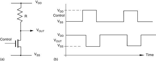
Figure 10.9 Resistor-NMOS transistor circuit (a) Circuit; (b) Waveform
When the control input to an NMOS transistor is connected to VSS, the transistor is turned OFF and acts like an OPEN switch; when the control input is connected to VDD, the transistor is turned ON and acts like a closed switch. Thus, the transistor functions in a similar manner to the switch. However, a switch is controlled by hand and can only be operated a few times a second, but a transistor’s control input can be driven by other transistors, allowing it to be operated millions of times a second.
Leave a Reply