
Before we take a look at some of the characteristics of “ideal” and “real” operational amplifiers it is important to define some of the terms and parameters that we apply to these devices.
11.3.1 Open-Loop Voltage Gain
The open-loop voltage gain of an operational amplifier is defined as the ratio of output voltage to input voltage measured with no feedback applied. In practice, this value is exceptionally high (typically greater than 100,000) but is liable to considerable variation from one device to another.
Open-loop voltage gain may thus be thought of as the “internal” voltage gain of the device, thus:

where AV(OL) is the open-loop voltage gain, VOUT and VIN are the output and input voltages respectively under open-loop conditions.
In linear voltage amplifying applications, a large amount of negative feedback will normally be applied and the open-loop voltage gain can be thought of as the internal voltage gain provided by the device.
The open-loop voltage gain is often expressed in decibels (dB) rather than as a ratio. In this case:
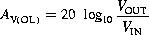
Most operational amplifiers have open-loop voltage gains of 90 dB, or more.
11.3.2 Closed-Loop Voltage Gain
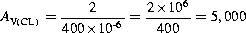
The closed-loop voltage gain of an operational amplifier is defined as the ratio of output voltage to input voltage measured with a small proportion of the output fed back to the input (i.e., with feedback applied). The effect of providing negative feedback is to reduce the loop voltage gain to a value that is both predictable and manageable. Practical closed-loop voltage gains range from one to several thousand but note that high values of voltage gain may make unacceptable restrictions on bandwidth.
Closed-loop voltage gain is once again the ratio of output voltage to input voltage but with negative feedback is applied, hence:

where AV(CL) is the open-loop voltage gain, VOUT and VIN are the output and input voltages respectively under closed-loop conditions. The closed-loop voltage gain is normally very much less than the open-loop voltage gain.
Example 11.1
An operational amplifier operating with negative feedback produces an output voltage of 2 V when supplied with an input of 400 μV. Determine the value of closed-loop voltage gain.
Solution
Now:

Thus:
Expressed in decibels (rather than as a ratio) this is:

11.3.3 Input Resistance
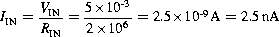
The input resistance of an operational amplifier is defined as the ratio of input voltage to input current expressed in ohms. It is often expedient to assume that the input of an operational amplifier is purely resistive though this is not the case at high frequencies where shunt capacitive reactance may become significant. The input resistance of operational amplifiers is very much dependent on the semiconductor technology employed. In practice values range from about 2 MΩ for common bipolar types to over 1012 Ω for FET and CMOS devices.
Input resistance is the ratio of input voltage to input current:

where RIN is the input resistance (in ohms), VIN is the input voltage (in volts) and IIN is the input current (in amps). Note that we usually assume that the input of an operational amplifier is purely resistive though this may not be the case at high frequencies where shunt capacitive reactance may become significant.
The input resistance of operational amplifiers is very much dependent on the semiconductor technology employed. In practice, values range from about 2 MΩ for bipolar operational amplifiers to over 1012 Ω for CMOS devices.
Example 11.2
An operational amplifier has an input resistance of 2 MΩ. Determine the input current when an input voltage of 5 mV is present.
Solution
Now:

thus,
11.3.4 Output Resistance
The output resistance of an operational amplifier is defined as the ratio of open-circuit output voltage to short-circuit output current expressed in ohms. Typical values of output resistance range from less than 10 Ω to around 100 Ω depending upon the configuration and amount of feedback employed.
Output resistance is the ratio of open-circuit output voltage to short-circuit output current, hence:
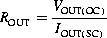
where ROUT is the output resistance (in ohms), VOUT(OC) is the open-circuit output voltage (in volts) and IOUT(SC) is the short-circuit output current (in amps).
11.3.4.1 Input Offset Voltage
An ideal operational amplifier would provide zero output voltage when 0 V difference is applied to its inputs. In practice, due to imperfect internal balance, there may be some small voltage present at the output. The voltage that must be applied differentially to the operational amplifier input in order to make the output voltage exactly zero is known as the input offset voltage.
Input offset voltage may be minimized by applying relatively large amounts of negative feedback or by using the offset null facility provided by a number of operational amplifier devices. Typical values of input offset voltage range from 1 mV to 15 mV. Where AC rather than DC coupling is employed, offset voltage is not normally a problem and can be happily ignored.
11.3.5 Full-Power Bandwidth
The full-power bandwidth for an operational amplifier is equivalent to the frequency at which the maximum undistorted peak output voltage swing falls to 0.707 of its low frequency (DC) value (the sinusoidal input voltage remaining constant). Typical full-power bandwidths range from 10 kHz to over 1 MHz for some high-speed devices.
11.3.6 Slew Rate
Slew rate is the rate of change of output voltage with time, when a rectangular step input voltage is applied (as shown in Figure 11.4). The slew rate of an operational amplifier is the rate of change of output voltage with time in response to a perfect step-function input.
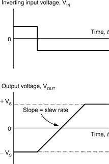
Figure 11.4 Slew rate for an operational amplifier
Hence:
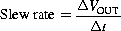
where ΔVOUT is the change in output voltage (in volts) and —t is the corresponding interval of time in s).
Slew rate is measured in V/s (or V/μs) and typical values range from 0.2 V/μs to over 20 V/μs. Slew rate imposes a limitation on circuits in which large amplitude pulses rather than small amplitude sinusoidal signals are likely to be encountered.
Leave a Reply