The three basic configurations for operational voltage amplifiers, together with the expressions for their voltage gain, are shown in Figure 11.7. Supply rails have been omitted from these diagrams for clarity but are assumed to be symmetrical about 0 V.
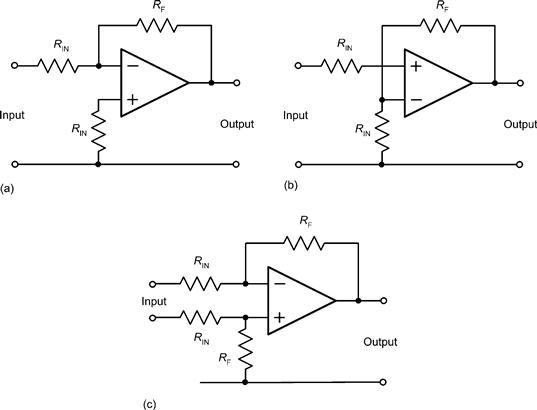
Figure 11.7 The three basic configurations for operational voltage amplifiers. (a) Inverting amplifier; (b) Non-inverting amplifier; (c) Differential amplifier.
All of the amplifier circuits described previously have used direct coupling and thus have frequency response characteristics that extend to DC. This, of course, is undesirable for many applications, particularly where a wanted AC signal may be superimposed on an unwanted DC voltage level or when the bandwidth of the amplifier greatly exceeds that of the signal that it is required to amplify. In such cases, capacitors of appropriate value may be inserted in series with the input resistor, RIN, and in parallel with the feedback resistor, RF, as shown in Figure 11.8.
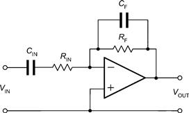
Figure 11.8 Adding capacitors to modify the frequency response of an inverting operational amplifier
The value of the input and feedback capacitors, CIN and CF, respectively, are chosen so as to roll-off the frequency response of the amplifier at the desired lower and upper cut-off frequencies, respectively. The effect of these two capacitors on an operational amplifier’s frequency response is shown in Figure 11.9.
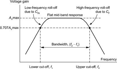
Figure 11.9 Effect of adding capacitors, CIN and CF, to modify the frequency response of an operational amplifier
By selecting appropriate values of capacitor, the frequency response of an inverting operational voltage amplifier may be very easily tailored to suit a particular set of requirements.
The lower cut-off frequency is determined by the value of the input capacitance, CIN, and input resistance, RIN. The lower cut-off frequency is given by:
where f1 is the lower cut-off frequency in Hz, CIN is in farads and RIN is in ohms.
Provided the upper frequency response is not limited by the gain×bandwidth product, the upper cut-off frequency will be determined by the feedback capacitance, CF, and feedback resistance, RF, such that:
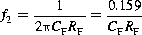
where f2 is the upper cut-off frequency in Hz, CF is in farads and R2 is in ohms.
Example 11.6
An inverting operational amplifier is to operate according to the following specification:
Voltage gain=100
Input resistance (at mid-band)=10 kW
Lower cut-off frequency=250 Hz
Upper cut-off frequency=15 kHz
Devise a circuit to satisfy the above specification using an operational amplifier.
Solution
To make things a little easier, we can break the problem down into manageable parts. We shall base our circuit on a single operational amplifier configured as an inverting amplifier with capacitors to define the upper and lower cut-off frequencies, as shown in the previous figure.
The nominal input resistance is the same as the value for RIN. Thus:

To determine the value of RF we can make use of the formula for mid-band voltage gain:

Thus, R2=Av×R1=100×10 kW=100 kW
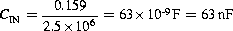
To determine the value of CIN we will use the formula for the low-frequency cut-off:

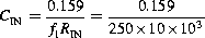
hence:
Finally, to determine the value of CF we will use the formula for high-frequency cut-off:

from which:
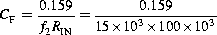
hence:
For most applications the nearest preferred values (68 nF for CIN and 100 pF for CF) would be perfectly adequate. The complete circuit of the operational amplifier stage is shown in Figure 11.10.
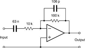
Figure 11.10 See Example 11.6. This operational amplifier has a mid-band voltage gain of 10 over the frequency range 250 Hz to 15 kHz
Leave a Reply