
The two main problems which face designers who have to integrate analog and digital circuits on the same printed circuit board (PCB) are:
• preventing digital switching noise from contaminating the analog signal, and
• interfacing the wide range of analog input voltages to the digital circuit.
Generating analog outputs from digital signals is not usually a problem. Generating digital inputs from analog signals is.
13.1.1 Ground Noise
The high-frequency switching noise discussed earlier must be kept out of analog circuits at all costs. An analog-to-digital interface quantizes a variable analog signal into a digital word, and the number of bits in the word determines the resolution that can be achieved of the signal. Assuming a full-scale voltage range of 0 to 10 V, which is typical of many analog-digital converters (ADCs), Table 13.1 shows the voltage levels that correspond to one bit change in the digital word.
Table 13.1
ADC resolution voltage for different word lengths, 10 V full-scale
| Word length | Resolution voltage |
| 8 bit | 39 mV |
| 10 bit | 10 mV |
| 12 bit | 2.4 mV |
| 14 bit | 0.6 mV |
| 16 bit | 0.15 mV |
You can see that the more resolution is demanded of the interface, the smaller the voltage change that will cause one bit change. 8 bits is regarded as commonplace in ADC circuits, 12 bits as reasonably high resolution (0.025%) and 16 bits as precision.
The significance of these diminishing voltage levels is that any noise that is coupled into the analog input will cause unwanted fluctuation of the digital value. For a 12-bit converter, a 1-bit uncertainty will be given by noise of 2.4 mV at the converter input; for a 16-bit, this reduces to 150 microvolts. By contrast, the switching noise on the digital ground line is normally tens of millivolts and frequently hundreds of millivolts peak amplitude. If this noise were coupled into the converter input—and it is hard to keep ground noise out of the input—you would be unable to use a converter of greater precision than 8–10 bits.
13.1.2 Filtering
One partial solution to this problem is to filter the bandwidth of the analog signal to well below that of the noise so that the effective noise signal is reduced. For slowly-varying analog signals this works reasonably well, especially if the noise injection occurs at the input of the signal-processing amplifier so that bandwidth limitation has maximum effect. Filtering is in any case good practice to minimize susceptibility to external noise.
Filtering the input amplifier is no use if the noise is injected into the ADC itself. For fast ADCs and wide-bandwidth analog signals you cannot take this approach anyway and the only available solution is to prevent the injection of digital noise at its source.
13.1.3 Segregation
The basic rule to follow when designing an analog-to-digital interface is to segregate the circuits, including grounds, completely. This means that:
• separate analog and digital grounds should be established, connected only at one point;
• the analog and digital sections of the circuit should be physically separated, with no digital tracks traversing the analog section or vice versa. This will minimize crosstalk between the circuits.
It should be appreciated that no grounding scheme which establishes a multiplicity of different grounds can ever be optimum, because there will always be circuits which need to communicate signals across different ground areas. These signals are then particularly exposed to the nuances of both internal and external interference, or indeed may be the source of it. You should always strive to make such circuits low-risk in terms of their bandwidth and sensitivity, or else keep a single ground system for all circuits (both digital and analog) and take extreme care in its layout so that ground noise from one noisy part of the system does not circulate in another sensitive part.
13.1.4 Single-Board Systems
The appropriate grounding schemes for single-board and multi-board systems are shown in Figure 13.1. If your system has a single analog-to-digital converter, perhaps with a multiplexer to select from several analog inputs, then the connection between analog and digital grounds can be made at this ADC as in Figure 13.1(a). This scheme requires that the analog and digital power supply returns are not linked together anywhere else, so that two separate power supply circuits are needed. The analog and digital grounds must be treated as entirely separate tracks, despite being nominally at the same potential; unavoidable noise currents circulating in the digital ground will then not couple into the “clean” analog ground. The digital ground should be of gridded or ground plane construction, whereas the analog section may benefit from a single-point grounding system, or may have a separate ground plane of its own. On no account should you extend the digital ground plane over the analog section of the board, since there will then be capacitive coupling from one ground plane to another.
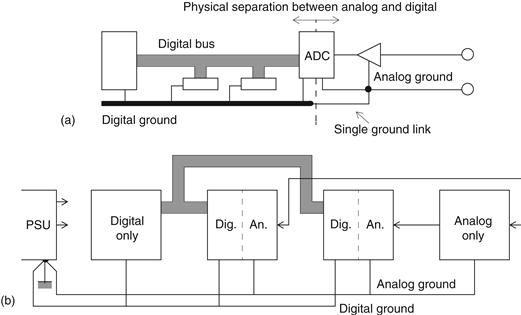
Figure 13.1 Layout for separate analog and digital grounds (a) Single-board;(b) Multi-board
13.1.5 Multi-Board Systems
When your system consists of several boards, some entirely digital, some entirely analog and some a mixture of the two, with an external power supply, then you cannot make the connection between digital and analog grounds at the ADC. There may be several ADCs in the one system. Instead, make the link at the power supply (Figure 13.1(b)) and run separate analog and digital grounds to each board that requires them. Digital-only boards should be located physically closer to the power supply to minimize the radiating loop area or length.
Leave a Reply