
PV modules are designed for outdoor use in such harsh conditions as marine, tropic, arctic, and desert environments. The choice of the photovoltaically active material can have important effects on system design and performance. Both the composition of the material and its atomic structure are influential. Photovoltaic materials include silicon, gallium arsenide, copper indium diselenide, cadmium telluride, indium phosphide, and many others. The atomic structure of a PV cell can be a single crystal, polycrystalline, or amorphous. The most commonly produced PV material is crystalline silicon, either single crystal or polycrystalline.
Cells are normally grouped into modules, which are encapsulated with various materials in order to protect the cells and the electrical connectors from the environment (Hansen et al., 2000). As shown in Figure 9.11, PV cell modules consist of NPM parallel branches and each branch has NSM solar cells in series. In the following analysis, superscript M refers to the PV module and superscript C refers to the solar cell. Therefore, as shown in Figure 9.11, the applied voltage at the module’s terminals is denoted by VM, whereas the total generated current is denoted by IM.
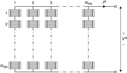
FIGURE 9.11 Schematic diagram of a PV module consisting of NPM parallel branches, each with NSM cells in series.
A model of the PV module can be obtained by replacing each cell in Figure 9.11 with the equivalent diagram from Figure 9.6. The model, developed by Lorenzo (1994), has the advantage that it can be used by applying only standard manufacturer-supplied data for the modules and the cells. The PV module current IM under arbitrary operating conditions can be described by:
![]() (9.19)
(9.19)
It should be noted that the PV module current, IM, is an implicit function, which depends on:
1. The short-circuit current of the module, given by:

2. The open-circuit voltage of the module, given by:

3. The equivalent series resistance of the module, given by:

4. The thermal voltage in the semiconductor of a single solar cell, given by:

The current practice dictates that the performance of a PV module is determined by exposing it at known standard rating conditions (SRCs) of irradiance, Gt,o = 1000 W/m2, and cell temperature, ![]() . These conditions are different from the nominal operating cell temperature (NOCT), as indicated in Table 9.1.
. These conditions are different from the nominal operating cell temperature (NOCT), as indicated in Table 9.1.
Table 9.1
9.2.1 PV arrays
The modules in a PV system are usually connected in arrays. An array with MP parallel branches each with MS modules in series is shown in Figure 9.12. By using a superscript A to denote array characteristics, the applied voltage at the array’s terminals is donated VA, whereas the total current of the array is denoted IA, given by:
![]() (9.20)
(9.20)
If it is assumed that the modules are identical and the ambient irradiance is the same in all modules, then the array’s current is given by:
EXAMPLE 9.3
A PV system is required to produce 250 W at 24 V. Using the solar cells of Example 9.2, design the PV panel, working at the maximum power point, if each cell is 9 cm2 in area.
Solution
From Example 9.2, Vmax = 0.526 V. The current density at maximum power point is 238.3 A/m2. Therefore, for the current cell,

This yields a power per cell = 0.526 × 0.2145 = 0.1 W.
Number of cells required = 250/0.1 = 2500.
Number of cells in series = system voltage/voltage per cell = 24/0.526 = 45.6 ≈ 46 (in fact with 46 cells, Voltage = 24.2 V).
Number of rows of 46 cells each, connected in parallel = 2500/46 = 54.3 ≈ 55 (in fact this panel yields 55 × 46 × 0.1 = 253 W).
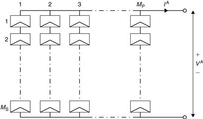
FIGURE 9.12 Cell array consisting of MP parallel branches, each with MS modules in series.
PV cells are fragile and susceptible to corrosion by humidity or fingerprints and can have delicate wire leads. Also, the operating voltage of a single PV cell is about 0.5 V, making it unusable for many applications. A module is a collection of PV cells that provides a usable operating voltage and offers means that protects the cells. Depending on the manufacturer and the type of PV material, modules have different appearances and performance characteristics. Also, modules may be designed for specific conditions, such as hot and humid, desert, or frozen climates. Usually, the cells are series connected to other cells to produce an operating voltage around 30–60 V. These strings of cells are then encapsulated with a polymer, a front glass cover, and a back material. Also, a junction box is attached at the back of the module for convenient wiring to other modules or other electrical equipment.
9.2.2 Types of PV technology
Many types of PV cells are available today. The main types are crystalline silicon, which accounts for roughly 80% of the PV market; thin-films, which have expanded to around 20% market share; and triple-junction cells, which are used in the emerging field of concentrating PV. This section gives details of commercialized flat-plate PV technologies and an overview of the cells that are currently in the research and development stage. Concentrating PV is discussed in section 9.7.
The choice between crystalline or thin-film PV modules for a given project depends heavily on climate and space. As we shall see below, crystalline modules are more efficient (i.e., give greater power output per unit area of module), while thin-film modules tend to have higher yield (i.e., give greater energy production for a given power rating)—especially in high temperatures (RENI, 2012). Assuming the same module price ($/W), crystalline modules are thus suited to space-constrained projects in moderate climates, and thin-film to hot climates and abundant space.
• Monocrystalline silicon cells. These cells are made from pure monocrystalline silicon. In these cells, the silicon has a single continuous crystal lattice structure with almost no defects or impurities. The main advantage of monocrystalline cells is their high efficiency, which is typically around 14–15%. Premium modules are available in the market with efficiencies just over 20% (RENI, 2012).
A disadvantage of these cells is the complicated manufacturing process that leads to relatively high costs, although greater production capacity of its raw material has decreased its price markedly in recent years, making it (and multicrystalline silicon) more price-competitive with thin-film modules. Compared to thin-film technologies, the power output of crystalline silicon decreases more rapidly with increasing cell temperature—its temperature coefficient is around minus 0.4–0.5%/°C. Additionally, the efficiency of crystalline silicon decreases somewhat in low light conditions, whereas the efficiency of thin-film modules remains roughly constant (Marion, 2008). Being relatively expensive, monocrystalline modules are most often used where the most possible power is required from a confined space, such as residential and commercial rooftops.
• Multicrystalline silicon cells. Multicrystalline cells, also known as polycrystalline cells, are produced using numerous grains of monocrystalline silicon. In the manufacturing process, molten polycrystalline silicon is cast into ingots, which are subsequently cut into very thin wafers and assembled into complete cells. Multicrystalline cells are cheaper to produce than monocrystalline ones because of the simpler manufacturing process required. They are, however, slightly less efficient, with typical module efficiencies around 13–15% (Price and Margolis, 2010) and high-end products up to 17% (RENI, 2010). They share monocrystalline cells’ relatively high temperature coefficient. With a long track record, high efficiency and moderate cost, multicrystalline modules are widely used in a wide variety of applications including roof- and ground-mounted arrays.
• Amorphous silicon. The general characteristics of amorphous silicon solar cells are given in Chapter 1, Section 1.5.1. Unlike mono- and multicrystalline cells, the silicon atoms in amorphous silicon (a-Si) cells are arranged in a thin homogenous layer. Amorphous silicon absorbs light more effectively than crystalline silicon, which leads to thinner cells, giving rise to the name thin film photovoltaics.
Advantages of these cells are their low manufacturing cost and high energy production per rated power capacity (kWh/kWp). The high yield stems from two attributes (Jardine et al., 2001; Kullmann, 2009):
1. Of all mass-market PV technologies, a-Si is the least impacted by heat, with a temperature coefficient of only around -0.2%/°C (Marion, 2008).
2. Amorphous silicon is relatively effective at absorbing the blue wavelengths of light that are encountered in cloudy conditions. Thus over the course of a year a-Si modules will generally produce more electricity than crystalline silicon ones of the same peak power, especially in warm climates.
The efficiency of a-Si modules is only 6–7% (Price and Margolis, 2010). Because of their low cost they are applied in a wide variety of PV systems; however, they face increasing competition from other thin-film technologies with higher efficiencies (see the following two types below). To increase their efficiency, a-Si is increasingly combined with layers of multicrystalline silicon or a variant, microcrystalline silicon. The properties of such “hybrid” modules lie between pure a-Si and crystalline silicon, with efficiencies around 9–10%. Some large PV manufacturers have phased out pure a-Si product lines and replaced them with hybrid designs. Perhaps the greatest advantage of these cells is that amorphous silicon can be deposited on a wide range of substrates, both rigid and flexible. Nowadays, the panels made from amorphous silicon solar cells come in a variety of shapes, such as roof tiles, which can replace normal ceramic tiles in a solar roof.
• Cadmium Telluride (CdTe). The thin-film PV market was largely developed by a single manufacturer, First Solar. It accounted for 59% of the global thin-film market in 2008 (Schreiber, 2009), as a result of achieving low cost (it was the first company to manufacture PV modules at less than $1 per Watt) and large production capacity (Runyon, 2012). Although the price advantage of CdTe has fallen with the emergence of low-cost crystalline silicon production in China, it retains a sizeable market presence with a manufacturing cost under $0.75/W (Runyon, 2012) and around 2 GW of annual production capacity.
Like amorphous silicon, CdTe is relatively tolerant to heat (its temperature coefficient is around minus 0.25–0.35%/°C), yet it has a higher efficiency of 10–11%. This combination of low cost, moderate efficiency, and large manufacturing volume has seen CdTe help create a new market for PV in recent years, that of utility-scale solar power plants. While CdTe modules are well suited to large ground-mounted arrays for commercial electricity production, they are also deployed on commercial rooftops.
• Copper Indium Gallium Selenide (CIGS). The most recent thin-film technology to be commercialized is the CIGS family. Like the other thin-films it can be manufactured at low cost and high volume in a continuous (as opposed to batch) manufacturing process. CIGS is also the main candidate for the commercial development of modules that do not use glass, making them flexible and very lightweight. Their electrical properties lie between crystalline silicon and CdTe, with conversion efficiency around 10–13% and moderate temperature coefficient of minus 0.3–0.4%/°C.
The moderate efficiency, low cost and light weight of CIGS make them ideally suited to rooftop installations, both residential and commercial. They are also a promising technology for building-integrated photovoltaic (BIPV) products. Numerous companies have been established to manufacture CIGS modules in recent years (Schreiber, 2009), although being new to the market they have not yet been deployed at the large scale of the other above-mentioned technologies (RENI, 2010).
• Thermophotovoltaics. These are photovoltaic devices that, instead of sunlight, use the infrared region of radiation, i.e., thermal radiation. A complete thermophotovoltaic (TPV) system includes a fuel, a burner, a radiator, a longwave photon recovery mechanism, a PV cell, and a waste heat recuperation system (Kazmerski, 1997). TPV devices convert radiation using exactly the same principles as photovoltaic devices, outlined in previous sections. The key differences between PV and TPV conversion are the temperatures of the radiators and the system geometries. In a solar cell, the radiation is received from the sun, which is at a temperature of about 6000 K and a distance of about 150 × 106 km. A TPV device, however, receives radiation, in either the broad or narrow band, from a surface at a much lower temperature of about 1300–1800 K and a distance of only a few centimeters. Although the blackbody power radiated by a surface varies at the fourth power of the absolute temperature, the inverse square law dependence of the power received by the detectors dominates. Therefore, although the power received by a non-concentrator solar cell is on the order of 0.1 W/cm2, that received by a TPV converter is likely to be 5–30 W/cm2, depending on the radiator temperature. Consequently, the power density output from a TPV converter is expected to be significantly greater than that from a non-concentrator PV converter. More details on TPVs can be found in the article by Coutts (1999).
Under development are polymer and organic solar cells. The attraction of these technologies is that they potentially offer fast production at low cost in comparison to crystalline silicon technologies, yet they typically have lower efficiencies, around 5% (Price and Margolis, 2010), and despite the demonstration of operational lifetimes and dark stabilities under inert conditions for thousands of hours, they suffer from stability and degradation problems. Organic materials are attractive, primarily due to the prospect of high-output manufacture using reel-to-reel or spray deposition. Other attractive features are the possibilities for ultrathin, flexible devices, which may be integrated into appliances or building materials, and tuning of color through the chemical structure (Nelson, 2002).
Another type of device being developed is the nano-PV, considered the third-generation PV; the first generation is the crystalline silicon cells, and the second generation thin-films. Instead of conductive materials and a glass substrate, nano-PV technologies rely on coating or mixing “printable” and flexible polymer substrates with electrically conductive nano-materials. This type of photovoltaics is expected to be commercially available within the next few years, reducing tremendously the cost of PV cells.
Leave a Reply