The implementations of the NOT and BUF gates shown above illustrate an important point, which is that it is generally easier to implement an inverting function than its non-inverting equivalent. In the same way that a NOT is easier to implement than a BUF, a NAND is easier to implement than an AND, and a NOR is easier to implement than an OR. More significantly, inverting functions typically require fewer transistors and operate faster than their non-inverting counterparts. This can obviously be an important design consideration. Consider a 2-input NAND gate, which requires four transistors (Figure 10.23). (Note that a 3-input version could be constructed by adding an additional PMOS transistor in parallel with Tr1 and Tr2, and an additional NMOS transistor in series with Tr3 and Tr4.)
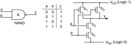
Figure 10.23 CMOS implementation of a 2-input NAND gate
When both a and b are presented with logic 1s, transistors Tr1 and Tr2 are turned OFF, transistors Tr3 and Tr4 are turned ON, and output y is connected to logic 0 via Tr3 and Tr4. Any other combination of inputs results in one or both of Tr3 and Tr4 being turned OFF, one or both of Tr1 and Tr2 being turned ON, and output y being connected to logic 1 via Tr1 and/or Tr2. Once again, it may help to visualize the gate’s operation in terms of switches rather than transistors (Figure 10.24).
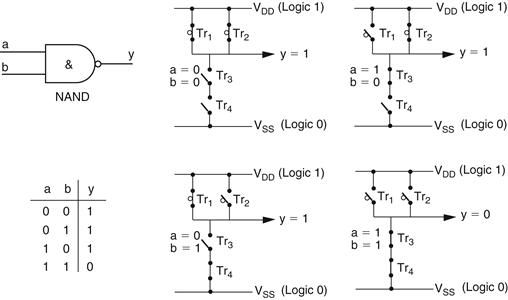
Figure 10.24 NAND gate’s operation represented in terms of switches
Now consider an AND gate. This is formed by inverting the output of a NAND with a NOT, which means that a 2-input AND requires six transistors (Figure 10.25).
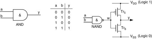
Figure 10.25 CMOS implementation of a 2-input AND gate
Leave a Reply