
The function of a modulator, as has been shown, is to superimpose the baseband signals on to a carrier while the demodulator provides the reverse role by extracting a carrier, known as the intermediate frequency, and leaving the baseband.
There are many modulators and demodulators commercially sold on the market as integrated chips or as part of a front end receiver chip containing other stages such as the tuner and detector. However, it is informative to look at the balanced modulator which is used in the majority of AM and other circuits.
A common method of obtaining a single sideband wave is illustrated in Figure 19.7. The output of this circuit differs from a conventional AM output in that it does not include the original radio frequency signal, but only the two sidebands. The single sideband is obtained by a highly selective filter.
An integrated circuit which is commonly used is the Philips MC 1496. This is a modulator/demodulator chip which uses a monolithic transistor array. It has many applications such as AM and suppressed carrier modulators, AM and FM demodulators and phase detectors. The basic theory of operation is shown in the data sheets at the end of this chapter. Figures 19.8 and 19.9 show the application of this chip as an AM modulator and demodulator, respectively.
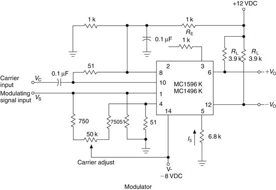
Figure 19.8 AM modulator
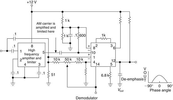
Figure 19.9 Demodulator
The AM modulator shown in Figure 19.8 allows no carrier at the output; by adding a variable offset voltage to the differential pairs at the carrier input the carrier level changes and its amplitude is determined by the AM modulation.
The frequency spectrum is shown in the data sheets; it can be seen that undesired sidebands appear if the modulation or carrier levels are high. These need to be filtered and a fourth-order Butterworth is ideal. Note also that the modulation levels may be varied by means of RE connected between pins 2 and 3 in Figure 19.8.
As can be seen from equation (1) in the data sheets, the output of the balanced modulator is a cosine function of the phase between the signal and carrier inputs. If the carrier input is driven hard enough, a switching action occurs and the output becomes a function of the input voltage. The output amplitude is maximized when the phase difference is zero.
A typical demodulator is shown in Figure 19.9. In this case the carrier is amplified by an intermediate frequency chip which provides a limited gain of 55 dB or higher at 400 μV. The carrier is then applied to the demodulator where the carrier frequency is attenuated. Output filtering is required to remove the high-frequency unwanted components.
Leave a Reply