
The first rule when you want to use a varying analog voltage to generate an on/off digital signal—as distinct from an analog-to-digital conversion—is: always use either a comparator or a Schmitt-trigger gate. Never feed an analog signal straight into an ordinary TTL or CMOS gate input.
The reason is that ordinary gates do not have well-defined input voltage switching thresholds. Not only that, but they are also very critical of slow rise-time inputs. Very few analog input signals have the slew rate, typically faster than 5 V/ms, required to produce a clean output from an ordinary logic gate. The result of applying a slow analog voltage to a logic gate is shown in Figure 13.2.

Figure 13.2 The effect of a slow input to a logic gate
A Schmitt trigger gate, or a comparator with hysteresis, will get over the slow rise time problem. A Schmitt trigger gate has the same output characteristics as an ordinary gate but it includes input hysteresis to ensure a fast transition. The threshold levels of typical Schmitt devices, such as the 74HC14, are specified within wide tolerances and so do not overcome the variability of the actual switching point. When the analog levels corresponding to high and low states can be kept above VIH and below VIL, respectively, a Schmitt is adequate. For more precision you will need to use a comparator with an accurately specified reference voltage.
Secondly, if the analog supply rail range is greater than the logic supply, interfacing the analog signal straight to the logic input will threaten the gate with damage. This is possible even if the normal signal range is within the logic supply range; abnormal conditions such as turn-on or turn-off may exceed the rails. This, of course, is also a problem with Schmitt trigger gates. Normally, the inputs are protected by clamp diodes to the supply and ground rails, but the current through these must be limited to a safe level so a resistor in series with the input is essential. More positive steps to limit the input voltage, such as running the analog section from the same supply voltage as the logic (heeding the earlier advice about separate digital and analog ground rails), are to be preferred.
13.2.1 Debouncing Switch Inputs
On the face of it, switch inputs to digital circuitry must be the easiest of interfaces. All you should need are an input port or gate, a pull-up resistor and a single pole switch (Figure 13.3). This circuit, though it undoubtedly works, is prone to a serious problem because of the electromechanical nature of the switch and the speed of logic devices.

Figure 13.3 Contact bounce
When a switch contact operates, the current flow is not cleanly initiated or interrupted. As the contacts come together or part, the instantaneous contact resistance varies due to contamination, and the mating surfaces may “bounce” apart a few times due to the springiness of the material. As a result the switching edge is irregular and may easily consist of several discrete edges, extending over a period of typically 1 ms. You can verify this behavior simply by observing the input waveform of Figure 13.3 on a storage scope.
Of course, the digital input responds very fast to each crossing of the switching threshold, and consequently the port or gate sees several transitions each time the switch is operated, before it settles to a steady-state 1 or 0. This may not be a problem for level-sensitive inputs, but it undoubtedly is for edge-sensitive ones such as counter or latch clock inputs. Mistriggering of counter circuits that are fed from a switch input is commonly caused by this phenomenon.
The simple solution to contact bounce is to filter the logic input with an RC network (Figure 13.4(a)). The RC time constant must be significantly longer than the bounce period to effectively attenuate the contact noise. This has the extra advantage of protecting against induced impulsive or RF interference, but it requires additional discrete components and demands that the logic input must be a Schmitt-trigger type, since the input rise time has been deliberately slowed.
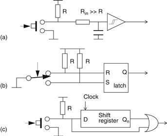
Figure 13.4 Switch de bouncing circuits
If the switch input may change state quickly, an RC time constant which is sufficiently long to cure the bounce will slow the response to the switch unacceptably. This can be overcome in two ways: the R-S latch, Figure 13.4(b), which requires a changeover rather than single-throw switch, or a software- or hardware-implemented delay. Figure 13.4(c) shows the hardware delay, which uses a continuously-clocked shift register and OR gate to effectively “window out” the bounce. The delay can be adjusted to suit the bounce period. These two solutions are most suited to realization with semi-custom logic arrays or ASICs, where the overhead of the extra logic is low.
Leave a Reply