
shows the circuit of an inverting amplifier with negative feedback applied. For the sake of our explanation we will assume that the operational amplifier is “ideal.” Now consider what happens when a small positive input voltage is applied. This voltage (VIN) produces a current (IIN) flowing in the input resistor R1.
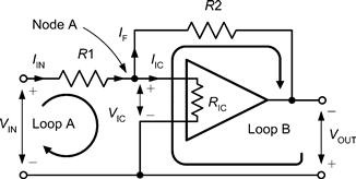
Figure 11.6 Operational amplifier with negative feedback applied
Since the operational amplifier is “ideal” we will assume that:
(a) the input resistance (i.e., the resistance that appears between the inverting and non-inverting input terminals, RIC) is infinite, and
(b) the open-loop voltage gain (i.e., the ratio of VOUT to VIN with no feedback applied) is infinite.
As a consequence of (a) and (b):
(i) the voltage appearing between the inverting and non-inverting inputs (VIC) will be zero, and
(ii) the current flowing into the chip (IIC) will be zero (recall that IIC=VIC/RIC and RIC is infinite).
Applying Kirchhoff’s Current Law at node A gives:
![]() (11.1)
(11.1)
(This shows that the current in the feedback resistor, R2, is the same as the input current, IIN).
Applying Kirchhoff’s Voltage Law to loop A gives:
![]() (11.2)
(11.2)
Using Kirchhoff’s Voltage Law in loop B gives:
![]() (11.3)
(11.3)
Combining (11.1) and (11.3) gives:
![]() (11.4)
(11.4)
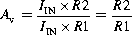
The voltage gain of the stage is given by:
![]() (11.5)
(11.5)
Combining (11.4) and (11.2) with (11.5) gives:
To preserve symmetry and minimize offset voltage, a third resistor is often included in series with the non-inverting input. The value of this resistor should be equivalent to the parallel combination of R1 and R2. Hence:

From this point onward (and to help you remember the function of the resistors), we shall refer to the input resistance as RIN and the feedback resistance as RF (instead of the more general and less meaningful R1 and R2, respectively).
Leave a Reply