
The output signal from the sensor of a measurement system or the signal from the control unit might have to be processed in some way to make it suitable to operate the next element in the control system. For example, the signal may be too small and have to be amplified, be analog and have to be made digital, be digital and have to be made analog, be a resistance change and have to be made into a current change, be a voltage change and have to be made into a suitable size current change, be a pressure change and have to be made into a current change, etc. All these changes can be referred to as signal processing. For example, the output from a thermocouple is a very small voltage, a few millivolts. A signal processing module might then be used to convert this into a larger voltage and provide cold junction compensation (i.e., allow for the cold junction not being at 0°C).
The following are some examples of signal processing commonly encountered in control systems.
18.5.1 Resistance to Voltage Converter
Consider how the resistance change produced by a thermistor when subject to a temperature change can be converted into a voltage change. Figure 18.34 shows how a potential divider circuit can be used. A constant voltage, of perhaps 6 V, is applied across the thermistor and another resistor in series. With a thermistor with a resistance of 4.7 kΩ, the series resistor might be 10 kΩ. The output signal is the voltage across the 10 kΩ resistor. When the resistance of the thermistor changes, the fraction of the 6 V across the 10 kΩ resistor changes.
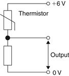
Figure 18.34 Resistance to voltage conversion for a thermistor
The output voltage is proportional to the fraction of the total resistance, which is between the output terminals. Thus:
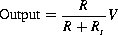
where V is the total voltage applied, in Figure 18.34 this is shown as 6 V, R the value of the resistance between the output terminals (10 kΩ) and Rt the resistance of the thermistor at the temperature concerned. The potential divider circuit is thus an example of a simple resistance to voltage converter. Another example of such a converter is the Wheatstone bridge.
18.5.2 Protection
An important element that is often required with signal processing is protection against high currents or high voltages. A high current can be protected against by the incorporation in the input line of a series resistor to limit the current to an acceptable level and a fuse to break if the current does exceed a safe level (Figure 18.35).
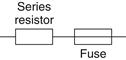
Figure 18.35 Protection against high currents
It is often so vital that high currents or high voltages are not transmitted from the sensor to a microprocessor that it may be necessary to completely isolate circuits so there are no electrical connections between them. This can be done using an optoisolator (Figure 18.36). Such a device converts an electrical signal into an optical signal, transmits it to a detector which then converts it back into an electrical signal. The input signal passes through an infrared light-emitting diode (LED) and so produces a beam of infrared radiation which is detected by a phototransistor.
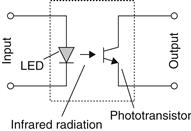
Figure 18.36 Optoisolator: infrared radiation is used to transmit signal from input to output circuit
18.5.3 Analog-to-Digital Conversion
The electrical output from sensors such as thermocouples, resistance elements used for temperature measurement, strain gauges, diaphragm pressure gauges, LVDTs, etc. is in analog form. An analog signal (Figure 18.37(a)) is one that is continuously variable, changing smoothly over a range of values. The signal is an analog, i.e., a scaled version, of the quantity it represents. A digital signal increases in jumps, being a sequence of pulses, often just on-off signals (Figure 18.37(b)). The value of the quantity instead of being represented by the height of the signal, as with analog, is represented by the sequence of on-off signals.
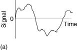
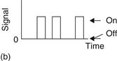
Figure 18.37 Signals: (a) analog; (b) digital
Microprocessors require digital inputs. Thus, where a microprocessor is used as part of a control system, the analog output from a sensor has to be converted into a digital form before it can be used as an input to the microprocessor. Thus there is a need for an analog-to-digital converter (ADC). Analog-to-digital conversion involves a number of stages. The first stage is to take samples of the analog signal (Figure 18.38(a)). A clock supplies regular time signal pulses (Figure 18.38(b)) to the analog-to-digital converter and every time it receives a pulse it samples the analog signal. The result is a series of narrow pulses with heights which vary in accord with the variation of the analog signal (Figure 18.38(c)). This sequence of pulses is changed into the signal form shown in Figure 18.38(d) by each sampled value being held until the next pulse occurs. This holding is necessary to allow time for the conversion to take place at an analog-to-digital converter. This converts each sample into a sequence of pulses representing the value. For example, the first sampled value might be represented by 101, the next sample by 011, etc. The 1 represents an “on” or “high” signal, the 0 an “off” or “low” signal. Analog-to-digital conversion thus involves a sample and hold unit followed by an analog-to-digital converter (Figure 18.39).
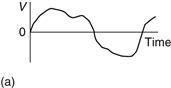
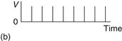
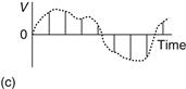
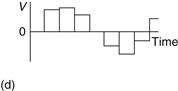
Figure 18.38 (a) Analog signal; (b) time signal; (c) sampled signal; (d) sampled and held signal
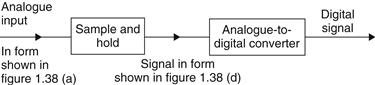
Figure 18.39 Analog-to-digital conversion
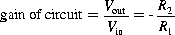
To illustrate the action of the analog-to-digital converter, consider one that gives an output restricted to three bits. The binary digits of 0 and 1, i.e., the “low” and “high” signals, are referred to as bits. A group of bits is called a word. Thus the three bits give the word length for this particular analog-to-digital converter. The word is what represents the digital version of the analog voltage. With three bits in a word we have the possible words of:

There are eight possible words which can be used to represent the analog input; the number of possible words with a word length of n bits is 2n. Thus we divide the maximum analog voltage into eight parts and one of the digital words corresponds to each. Each rise in the analog voltage of (1/8) of the maximum analog input then results in a further bit being generated. Thus for word 000 we have 0 V input. To generate the next digital word of 001 the input has to rise to 1/8 of the maximum voltage. To generate the next word of 010 the input has to rise to 2/8 of the maximum voltage. Figure 18.40 illustrates this conversion of the sampled and held input voltage to a digital output.
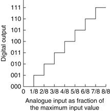
Figure 18.40 Digital output from an ADC
Thus if we had a sampled analog input of 8 V, the digital output would be 000 for a 0 V input and would remain at that output until the analog voltage had risen to 1 V, i.e., 1/8 of the maximum analog input. It would then remain at 001 until the analog input had risen to 2 V. This value of 001 would continue until the analog input had risen to 3 V. The smallest change in the analog voltage that would result in a change in the digital output is thus 1 V. This is termed the resolution of the converter.
The word length possible with an analog-to-digital converter determines its resolution. With a word length of n bits the maximum, or full scale, analog input VFS is divided into 2n pieces. The minimum change in input that can be detected, i.e., the resolution, is thus VFS /2n. With an analog-to-digital converter having a word length of 10 bits and the maximum analog signal input range 10 V, then the maximum analog voltage is divided into 210=1024 pieces and the resolution is 10/1024=9.8 mV.
There are a number of forms of analog-to-digital converter; the most commonly used being successive approximations, dual-slope and flash. Successive approximations converters are probably the most widely used; dual slope converters have the advantage of excellent noise rejection and flash converters give the highest conversion rates.
18.5.4 Digital-to-Analog Conversion
The output from a microprocessor is digital. Most control elements require an analog input and so the digital output from a microprocessor has to be converted into an analog form before it can be used by them. The input to a digital-to-analog converter is a binary word and the output its equivalent analog value. For example, if we have a full scale output of 7 V then a digital input of 000 will give 0 V, 001 give 1 V … and 111 the full scale value of 7 V. Figure 18.41 illustrates this.
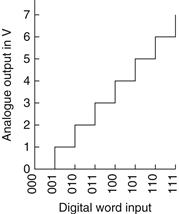
Figure 18.41 Digital-to-analog conversion
18.5.5 Amplifiers
The operational amplifier is the basis of many signal processing elements, the basic amplifier being supplied as an integrated circuit on a silicon chip. It has two inputs, termed the inverting input (-) and the noninverting input (+) and is a high gain DC amplifier, the gain typically being of the order of 100,000 or more. Figure 18.42 shows the pin connections for a 741 operational amplifier with the symbol for the operational amplifier. Pins 4 and 7 are for the connections to the supply voltage for the amplifier, pin 2 for the inverting input, pin 3 for the noninverting input. The output is taken from pin 6. Pins 1 and 5 are for the offset null. These are to enable circuits to be connected to enable corrections to be made for the nonideal behavior of the amplifier.
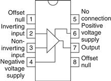
Figure 18.42 Amplifier
Consider the amplifier when used as an inverting amplifier (Figure 18.43), i.e., an amplifier which gives an output, which is out-of-phase with respect to the input. For the circuit shown in Figure 18.43, the connections for the power supply and the offset null have been omitted. The input is connected to the inverting input, the noninverting input being connected to earth. A feedback loop is connected, via the resistor R2, to the inverting input. The output voltage of such an amplifier is limited to about ±10 V and thus, since the gain is about 100,000, the input voltage to the inverting input at X, Vx, must be between about +0.0001V and -0.0001V. This is virtually zero and so point X is at virtually earth potential. For this reason it is called a virtual earth. The potential difference across the input resistance R1 is (Vin–Vx) and thus (Vin–Vx)=I1R1. But Vx is virtually zero and so we can write:

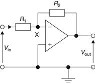
Figure 18.43 Inverting amplifier
Operational amplifiers have very high resistance between their input terminals; for example, the resistance with the 741 operational amplifier is about 2 MΩ. Thus virtually no current flows from point X through the inverting input and so to earth. Thus the current I1 that flows through R1 must be essentially the current flowing through R2. The potential difference across R2 is (Vx–Vout). Thus we can write (Vx–Vout).=I1R2. But as Vx is effectively zero, we can write:

Eliminating 11 from these two simultaneous equations gives:
The negative sign indicates that the output is 180° out-of-phase with the input. The gain is determined solely by the values of the two resistors. A noninverting amplifier can likewise be produced by taking the input to the noninverting input instead of the inverting input.
As an illustration of the use of an operational amplifier, consider Figure 18.44 which shows how it can be used as a differential amplifier to amplify the difference between two input voltages. Since there is virtually no current through the high resistance in the operational amplifier between the two input terminals, both the inputs X will be at the same potential. The voltage V2 is across resistors R1 and R2 in series. Thus, the potential Vx at X is:

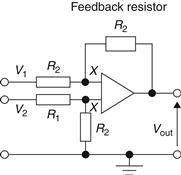
Figure 18.44 Differential amplifier
Since the operational amplifier has a very high input resistance, the current through the feedback resistance will be equal to that from V1 through R1. Hence, we have:
and so:
Hence, substituting for Vx using the earlier equation, gives:
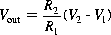
The output is a measure of the difference between the two input voltages.
More information on op-amps can be found in
The output signal from the sensor of a measurement system or the signal from the control unit might have to be processed in some way to make it suitable to operate the next element in the control system. For example, the signal may be too small and have to be amplified, be analog and have to be made digital, be digital and have to be made analog, be a resistance change and have to be made into a current change, be a voltage change and have to be made into a suitable size current change, be a pressure change and have to be made into a current change, etc. All these changes can be referred to as signal processing. For example, the output from a thermocouple is a very small voltage, a few millivolts. A signal processing module might then be used to convert this into a larger voltage and provide cold junction compensation (i.e., allow for the cold junction not being at 0°C).
The following are some examples of signal processing commonly encountered in control systems.
18.5.1 Resistance to Voltage Converter
Consider how the resistance change produced by a thermistor when subject to a temperature change can be converted into a voltage change. Figure 18.34 shows how a potential divider circuit can be used. A constant voltage, of perhaps 6 V, is applied across the thermistor and another resistor in series. With a thermistor with a resistance of 4.7 kΩ, the series resistor might be 10 kΩ. The output signal is the voltage across the 10 kΩ resistor. When the resistance of the thermistor changes, the fraction of the 6 V across the 10 kΩ resistor changes.
Figure 18.34 Resistance to voltage conversion for a thermistor
The output voltage is proportional to the fraction of the total resistance, which is between the output terminals. Thus:
where V is the total voltage applied, in Figure 18.34 this is shown as 6 V, R the value of the resistance between the output terminals (10 kΩ) and Rt the resistance of the thermistor at the temperature concerned. The potential divider circuit is thus an example of a simple resistance to voltage converter. Another example of such a converter is the Wheatstone bridge.
18.5.2 Protection
An important element that is often required with signal processing is protection against high currents or high voltages. A high current can be protected against by the incorporation in the input line of a series resistor to limit the current to an acceptable level and a fuse to break if the current does exceed a safe level (Figure 18.35).
Figure 18.35 Protection against high currents
It is often so vital that high currents or high voltages are not transmitted from the sensor to a microprocessor that it may be necessary to completely isolate circuits so there are no electrical connections between them. This can be done using an optoisolator (Figure 18.36). Such a device converts an electrical signal into an optical signal, transmits it to a detector which then converts it back into an electrical signal. The input signal passes through an infrared light-emitting diode (LED) and so produces a beam of infrared radiation which is detected by a phototransistor.
Figure 18.36 Optoisolator: infrared radiation is used to transmit signal from input to output circuit
18.5.3 Analog-to-Digital Conversion
The electrical output from sensors such as thermocouples, resistance elements used for temperature measurement, strain gauges, diaphragm pressure gauges, LVDTs, etc. is in analog form. An analog signal (Figure 18.37(a)) is one that is continuously variable, changing smoothly over a range of values. The signal is an analog, i.e., a scaled version, of the quantity it represents. A digital signal increases in jumps, being a sequence of pulses, often just on-off signals (Figure 18.37(b)). The value of the quantity instead of being represented by the height of the signal, as with analog, is represented by the sequence of on-off signals.
Figure 18.37 Signals: (a) analog; (b) digital
Microprocessors require digital inputs. Thus, where a microprocessor is used as part of a control system, the analog output from a sensor has to be converted into a digital form before it can be used as an input to the microprocessor. Thus there is a need for an analog-to-digital converter (ADC). Analog-to-digital conversion involves a number of stages. The first stage is to take samples of the analog signal (Figure 18.38(a)). A clock supplies regular time signal pulses (Figure 18.38(b)) to the analog-to-digital converter and every time it receives a pulse it samples the analog signal. The result is a series of narrow pulses with heights which vary in accord with the variation of the analog signal (Figure 18.38(c)). This sequence of pulses is changed into the signal form shown in Figure 18.38(d) by each sampled value being held until the next pulse occurs. This holding is necessary to allow time for the conversion to take place at an analog-to-digital converter. This converts each sample into a sequence of pulses representing the value. For example, the first sampled value might be represented by 101, the next sample by 011, etc. The 1 represents an “on” or “high” signal, the 0 an “off” or “low” signal. Analog-to-digital conversion thus involves a sample and hold unit followed by an analog-to-digital converter (Figure 18.39).
Figure 18.38 (a) Analog signal; (b) time signal; (c) sampled signal; (d) sampled and held signal
Figure 18.39 Analog-to-digital conversion
To illustrate the action of the analog-to-digital converter, consider one that gives an output restricted to three bits. The binary digits of 0 and 1, i.e., the “low” and “high” signals, are referred to as bits. A group of bits is called a word. Thus the three bits give the word length for this particular analog-to-digital converter. The word is what represents the digital version of the analog voltage. With three bits in a word we have the possible words of:
There are eight possible words which can be used to represent the analog input; the number of possible words with a word length of n bits is 2n. Thus we divide the maximum analog voltage into eight parts and one of the digital words corresponds to each. Each rise in the analog voltage of (1/8) of the maximum analog input then results in a further bit being generated. Thus for word 000 we have 0 V input. To generate the next digital word of 001 the input has to rise to 1/8 of the maximum voltage. To generate the next word of 010 the input has to rise to 2/8 of the maximum voltage. Figure 18.40 illustrates this conversion of the sampled and held input voltage to a digital output.
Figure 18.40 Digital output from an ADC
Thus if we had a sampled analog input of 8 V, the digital output would be 000 for a 0 V input and would remain at that output until the analog voltage had risen to 1 V, i.e., 1/8 of the maximum analog input. It would then remain at 001 until the analog input had risen to 2 V. This value of 001 would continue until the analog input had risen to 3 V. The smallest change in the analog voltage that would result in a change in the digital output is thus 1 V. This is termed the resolution of the converter.
The word length possible with an analog-to-digital converter determines its resolution. With a word length of n bits the maximum, or full scale, analog input VFS is divided into 2n pieces. The minimum change in input that can be detected, i.e., the resolution, is thus VFS /2n. With an analog-to-digital converter having a word length of 10 bits and the maximum analog signal input range 10 V, then the maximum analog voltage is divided into 210=1024 pieces and the resolution is 10/1024=9.8 mV.
There are a number of forms of analog-to-digital converter; the most commonly used being successive approximations, dual-slope and flash. Successive approximations converters are probably the most widely used; dual slope converters have the advantage of excellent noise rejection and flash converters give the highest conversion rates.
18.5.4 Digital-to-Analog Conversion
The output from a microprocessor is digital. Most control elements require an analog input and so the digital output from a microprocessor has to be converted into an analog form before it can be used by them. The input to a digital-to-analog converter is a binary word and the output its equivalent analog value. For example, if we have a full scale output of 7 V then a digital input of 000 will give 0 V, 001 give 1 V … and 111 the full scale value of 7 V. Figure 18.41 illustrates this.
Figure 18.41 Digital-to-analog conversion
18.5.5 Amplifiers
The operational amplifier is the basis of many signal processing elements, the basic amplifier being supplied as an integrated circuit on a silicon chip. It has two inputs, termed the inverting input (-) and the noninverting input (+) and is a high gain DC amplifier, the gain typically being of the order of 100,000 or more. Figure 18.42 shows the pin connections for a 741 operational amplifier with the symbol for the operational amplifier. Pins 4 and 7 are for the connections to the supply voltage for the amplifier, pin 2 for the inverting input, pin 3 for the noninverting input. The output is taken from pin 6. Pins 1 and 5 are for the offset null. These are to enable circuits to be connected to enable corrections to be made for the nonideal behavior of the amplifier.
Figure 18.42 Amplifier
Consider the amplifier when used as an inverting amplifier (Figure 18.43), i.e., an amplifier which gives an output, which is out-of-phase with respect to the input. For the circuit shown in Figure 18.43, the connections for the power supply and the offset null have been omitted. The input is connected to the inverting input, the noninverting input being connected to earth. A feedback loop is connected, via the resistor R2, to the inverting input. The output voltage of such an amplifier is limited to about ±10 V and thus, since the gain is about 100,000, the input voltage to the inverting input at X, Vx, must be between about +0.0001V and -0.0001V. This is virtually zero and so point X is at virtually earth potential. For this reason it is called a virtual earth. The potential difference across the input resistance R1 is (Vin–Vx) and thus (Vin–Vx)=I1R1. But Vx is virtually zero and so we can write:
Figure 18.43 Inverting amplifier
Operational amplifiers have very high resistance between their input terminals; for example, the resistance with the 741 operational amplifier is about 2 MΩ. Thus virtually no current flows from point X through the inverting input and so to earth. Thus the current I1 that flows through R1 must be essentially the current flowing through R2. The potential difference across R2 is (Vx–Vout). Thus we can write (Vx–Vout).=I1R2. But as Vx is effectively zero, we can write:
Eliminating 11 from these two simultaneous equations gives:
The negative sign indicates that the output is 180° out-of-phase with the input. The gain is determined solely by the values of the two resistors. A noninverting amplifier can likewise be produced by taking the input to the noninverting input instead of the inverting input.
As an illustration of the use of an operational amplifier, consider Figure 18.44 which shows how it can be used as a differential amplifier to amplify the difference between two input voltages. Since there is virtually no current through the high resistance in the operational amplifier between the two input terminals, both the inputs X will be at the same potential. The voltage V2 is across resistors R1 and R2 in series. Thus, the potential Vx at X is:
Figure 18.44 Differential amplifier
Since the operational amplifier has a very high input resistance, the current through the feedback resistance will be equal to that from V1 through R1. Hence, we have:
and so:
Hence, substituting for Vx using the earlier equation, gives:
The output is a measure of the difference between the two input voltages.
Leave a Reply